TikZ and PGF Manual
Libraries
49 Circuit Libraries
Written and documented by Till Tantau, and Mark Wibrow. Inspired by the work of Massimo Redaelli.
49.1 Introduction
The circuit libraries can be used to draw different kinds of electrical or logical circuits. There is not a single library for this, but a whole hierarchy of libraries that work in concert. The main design goal was to create a balance between ease-of-use and ease-of-extending, while creating high-quality graphical representations of circuits.
49.1.1 A First Example
                \usetikzlibrary {circuits.ee.IEC}

                \begin{tikzpicture}[circuit ee IEC,x=3cm,y=2cm,semithick,

                                    every info/.style={font=\footnotesize},

                                    small circuit symbols,

                                    set resistor graphic=var resistor IEC graphic,

                                    set diode graphic=var diode IEC graphic,

                                    set make contact graphic=
                var make contact IEC graphic]

                  % Let us start with some contacts:

                  \foreach \contact/\y in {1/1,2/2,3/3.5,4/4.5,5/5.5}

                  {

                    \node [contact] (left contact \contact) at
                (0,\y) {};

                    \node [contact] (right contact \contact) at
                (1,\y) {};

                  }

                  \draw (right contact 1) --
                (right contact 2) --
                (right contact 3)

                     --
                (right contact 4) --
                (right contact 5);


                  \draw (left contact 1) to
                [diode] ++(down:1)

                                         to
                [voltage source={near start,

                                                               direction
                  info={volt=3}},

                                             resistor={near end,ohm=3}] ++(right:1)

                                         to
                (right contact 1);

                  \draw (left contact 1) to
                [resistor={ohm=4}] (right contact 1);

                  \draw (left contact 1) to
                [resistor={ohm=3}] (left contact 2);

                  \draw (left contact 2) to
                [voltage source={near start,

                                                               direction
                  info={<-,volt=8}},

                                             resistor={ohm=2,near end}] (right contact 2);

                  \draw (left contact 2) to
                [resistor={near start,ohm=1},

                                             make contact={near end,info'={[red]$S_1$}}]

                                         (left contact 3);

                  \draw (left contact 3) to
                [current direction'={near start,info=$\iota$},

                                             resistor={near end,info={$R=4\Omega$}}]

                                         (right contact 3);

                  \draw (left contact 4) to
                [voltage source={near start,

                                                               direction
                  info={<-,volt=8}},

                                             resistor={ohm=2,near end}] (right contact 4);

                  \draw (left contact 3) to
                [resistor={ohm=1}] (left contact 4);

                  \draw (left contact 4) to
                [resistor={ohm=3}] (left contact 5);

                  \draw (left contact 5) to
                [resistor={ohm=4}] (right contact 5);

                  \draw (left contact 5) to
                [diode] ++(up:1)

                                         to
                [voltage source={near start,

                                                               direction
                  info={volt=3}},

                                             resistor={near end,ohm=3}] ++(right:1)

                                         to
                (right contact 5);

                \end{tikzpicture}
An important feature of the circuits library is that the appearance of a circuit can be configured in general ways and that the labels are placed automatically by default. Here is the graphic once more, generated from exactly the same source code, with only the options of the {tikzpicture} environment replaced by [rotate=-90,circuit ee IEC,x=3.25cm,y=2.25cm]:
49.1.2 Symbols
A circuit typically consists of numerous electronic elements like logical gates or resistors or diodes that are connected by wires. In pgf/TikZ, we use nodes for the electronic elements and normal lines for the wires. TikZ offers a large number of different ways of positioning and connecting nodes in general, all of which can be used here. Additionally, the circuits library defines an additional useful to-path that is particularly useful for elements like a resistor on a line.
There are many different names that are used to refer to electrical “elements”, so a bit of terminology standardization is useful: We will call such elements symbols. A symbol shape is a pgf shape declared using the \pgfdeclareshape command. A symbol node is a node whose shape is a symbol shape.
49.1.3 Symbol Graphics
Symbols can be created by \node[shape=some symbol shape]. However, in order to represent some symbols correctly, just using standard pgf shapes is not sufficient. For instance, most symbols have a visually appealing “default size”, but the size of a symbol shape depends only on the current values of parameters like minimum height or inner xsep.
For these reasons, the circuit libraries introduce the concept of a symbol graphic. This is a style that causes a \node to not only have the correct shape, but also the correct size and the correct path usage. More generally, this style may set up things in any way so that the “symbol looks correct”. When you write, for instance, \node[diode], then the style called diode graphic is used, which in turn is set to something like shape=diode IEC,draw,minimum height=....
Here is an overview of the different kinds of circuit libraries:
-
• The TikZ-library circuits defines general keys for creating circuits. Mostly, these keys are useful for defining more specialized libraries.
You normally do not use this library directly since it does not define any symbol graphics.
-
• The TikZ-library circuits.logic defines keys for creating logical gates like and-gates or xor-gates. However, this library also does not actually define any symbol graphics; this is done by two sublibraries:
-
– The library circuits.logic.US defines symbol graphics that cause the logical gates to be rendered in the “US-style”. It includes all of the above libraries and you can use this library directly.
-
– The library circuits.logic.IEC also defines symbol graphics for logical gates, but it uses rectangular gates rather that the round US-gates. This library can coexist peacefully with the above library, you can change which symbol graphics are used “on the fly”.
-
-
• The TikZ-library circuits.ee defines keys for symbols from electrical engineering like resistors or capacitors. Again, sublibraries define the actual symbol graphics.
-
– The library circuits.ee.IEC defines symbol shapes that follow the IEC norm.
-
-
• The pgf-libraries shapes.gates.* define (circuit) symbol shapes. However, you normally do not use these shapes directly, rather you use a style that uses an appropriate symbol graphic, which in turn uses one of these shapes.
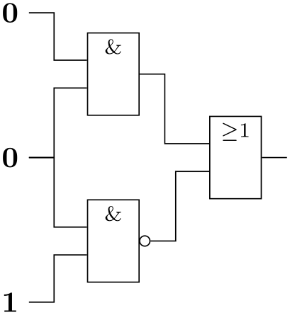
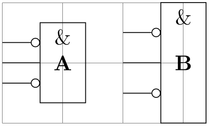
Let us have a look at a simple example. Suppose we wish to create a logical circuit. Then we first have to decide which symbol graphics we would like to use. Suppose we wish to use the US-style, then we would include the library circuits.logic.US. If you wish to use IEC-style symbols, use circuits.logic.IEC. If you cannot decide, include both:
\usetikzlibrary{circuits.logic.US,circuits.logic.IEC}
To create a picture that contains a US-style circuit you can now use the option circuit logic US. This will set up keys like and gate to create use an appropriate symbol graphic for rendering an and gate. Using the circuit logic IEC instead will set up and gate to use another symbol graphic.
                \usetikzlibrary {circuits.logic.US}

                \begin{tikzpicture}[circuit logic US]

                  \matrix[column sep=7mm]

                  {

                    \node (i0) {0}; &
                                           &
                \\

                                    &
                \node [and gate] (a1) {};  &
                \\

                    \node (i1) {0}; &
                                           &
                \node [or gate] (o) {};\\

                                    &
                \node [nand gate] (a2) {}; &
                \\

                    \node (i2) {1}; &
                                           &
                \\

                  };

                  \draw (i0.east) --
                ++(right:3mm) |-
                (a1.input 1);

                  \draw (i1.east) --
                ++(right:3mm) |-
                (a1.input 2);

                  \draw (i1.east) --
                ++(right:3mm) |-
                (a2.input 1);

                  \draw (i2.east) --
                ++(right:3mm) |-
                (a2.input 2);

                  \draw (a1.output) --
                ++(right:3mm) |-
                (o.input 1);

                  \draw (a2.output) --
                ++(right:3mm) |-
                (o.input 2);

                  \draw (o.output) --
                ++(right:3mm);

                \end{tikzpicture}
                \usetikzlibrary {circuits.logic.IEC}

                \begin{tikzpicture}[circuit logic IEC]

                  \matrix[column sep=7mm]

                  {

                    \node (i0) {0}; &
                                           &
                \\

                                    &
                \node [and gate] (a1) {};  &
                \\

                    \node (i1) {0}; &
                                           &
                \node [or gate] (o) {};\\

                                    &
                \node [nand gate] (a2) {}; &
                \\

                    \node (i2) {1}; &
                                           &
                \\

                  };

                  \draw (i0.east) --
                ++(right:3mm) |-
                (a1.input 1);

                  \draw (i1.east) --
                ++(right:3mm) |-
                (a1.input 2);

                  \draw (i1.east) --
                ++(right:3mm) |-
                (a2.input 1);

                  \draw (i2.east) --
                ++(right:3mm) |-
                (a2.input 2);

                  \draw (a1.output) --
                ++(right:3mm) |-
                (o.input 1);

                  \draw (a2.output) --
                ++(right:3mm) |-
                (o.input 2);

                  \draw (o.output) --
                ++(right:3mm);

                \end{tikzpicture}
49.1.4 Annotations
An annotation is a little extra drawing that can be added to a symbol. For instance, when you add two little parallel arrows pointing away from some electrical element, this usually means that the element is light emitting.
Instead of having one symbol for “diode” and another for “light emitting diode”, there is just one diode symbol, but you can add the light emitting annotation to it. This is done by passing the annotation as a parameter to the symbol as in the following example:
49.2 The Base Circuit Library
-
TikZ Library circuits 
\usetikzlibrary{circuits} %
LaTeX
and plain
TeX
\usetikzlibrary[circuits] % ConTeXt
This library is a base library that is included by other circuit libraries. You do not include it directly, but you will
typically use some of the general keys, described below.
-
/tikz/circuits(no value) 
This key should be passed as an option to a picture or a scope that contains a circuit. It will do some internal setups. This key is normally called by more specialized keys like circuit ee IEC.
49.2.1 Symbol Size
-
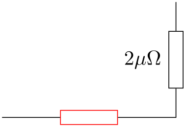
/tikz/circuit symbol unit=⟨dimension⟩ (no default, initially 7pt) 
This dimension is a “unit” for the size of symbols. The libraries generally define the sizes of symbols relative to this dimension. For instance, the longer side of an inductor is, by default, in the IEC library equal to five times this ⟨dimension⟩. When you change this ⟨dimension⟩, the size of all symbols will automatically change accordingly.
Note, that it is still possible to overwrite the size of any particular symbol. These settings apply only to the default sizes.
                    \usetikzlibrary {circuits.ee.IEC}

                    \begin{tikzpicture}[circuit ee IEC]

                      \draw (0,1) to
                    [resistor] (3.5,1);

                      \draw[circuit symbol unit=14pt]

                            (0,0) to [resistor] (3.5,0);

                    \end{tikzpicture}
-
/tikz/huge circuit symbols(style, no value) 
This style sets the default circuit symbol unit to 10pt.
-
/tikz/large circuit symbols(style, no value) 
This style sets the default circuit symbol unit to 8pt.
-
/tikz/medium circuit symbols(style, no value) 
This style sets the default circuit symbol unit to 7pt.
-
/tikz/small circuit symbols(style, no value) 
This style sets the default circuit symbol unit to 6pt.
-
/tikz/tiny circuit symbols(style, no value) 
This style sets the default circuit symbol unit to 5pt.
-
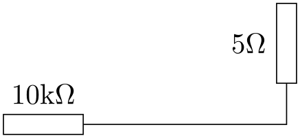
/tikz/circuit symbol size=width ⟨width⟩ height ⟨height⟩(no default) 
This key sets minimum height to ⟨height⟩ times the current value of the circuit symbol unit and the minimum width to ⟨width⟩ times this value. Thus, this option can be used with a node command to set the size of the node as a multiple of the circuit symbol unit.
                    \usetikzlibrary {circuits.ee.IEC}

                    \begin{tikzpicture}[circuit ee IEC]

                      \draw (0,1) to
                    [resistor] (2,1) to[inductor] (4,1);


                      \begin{scope}

                        [every resistor/.style={circuit symbol size=width 3 height 1}]

                        \draw (0,0) to
                    [resistor] (2,0) to[inductor] (4,0);

                      \end{scope}

                    \end{tikzpicture}
49.2.2 Declaring New Symbols
-
/tikz/circuit declare symbol=⟨name⟩(no default) 
-
1. The inner sep is set to 0.5pt.
-
2. The following style is executed:
-
/tikz/every circuit symbol(style, no value) 
Use this style to set up things in general.
-
-
3. The graphic options that have been set using set ⟨name⟩ graphic are set.
-
4. The style every ⟨name⟩ is executed. You can use it to configure the symbol further.
-
5. The ⟨options⟩ are executed.
This key is used to declare a symbol. It does not cause this symbol to be shown nor does it set a graphic to be used for the symbol, it simply “prepares” several keys that can later be used to draw a symbol and to configure it.
In detail, the first key that is defined is just called ⟨name⟩. This key should be given as an option to a node or on a to path, as explained below. The key will take options, which can be used to influence the way the symbol graphic is rendered.
Let us have a look at an example. Suppose we want to define a symbol called foo, which just looks like a simple rectangle. We could then say
The symbol could now be used like this:
However, in the above example we would not actually see anything since we have not yet set up the graphic to be used by foo. For this, we must use a key called set foo graphic or, generally, set ⟨name⟩ graphic. This key gets graphic options as parameter that will be set when a symbol foo should be shown:
\usetikzlibrary {circuits}
\begin{tikzpicture}
[circuit declare symbol=foo,
set foo graphic={draw,shape=rectangle,minimum size=5mm}]
                      \node [foo]       at
                    (1,1) {};

                      \node [foo={red}] at
                    (2,1) {};
\end{tikzpicture}
In detail, when you use the key ⟨name⟩=⟨options⟩ with a node, the following happens:
The key ⟨name⟩ will have a different effect when it is used on a to path command inside a circuit environment (the circuit environment sets up to paths in such a way that the use of a key declared using circuit declare symbol is automatically detected). When ⟨name⟩ is used on a to path, the above actions also happen (setting the inner separation, using the symbol graphic, and so on), but they are passed to the key circuit handle symbol, which is explained next.
-
/tikz/circuit handle symbol=⟨options⟩(no default) 
-
1. The to path is locally changed and set to an internal path (which you should not try to change) that consists mostly of a single straight line.
-
2. The ⟨options⟩ are tentatively executed with filtering switched on. Everything is filtered out, except for the key pos and also the styles at start, very near start, near start, midway, near end, very near end, and at end. If none of them is found, midway is used.
-
3. The filtered option is used to determine a position for the symbol on the path. At the given position (with pos=0 representing the start and pos=1 representing the end), a node will be added to the path (in a manner to be described presently).
-
4. This node gets ⟨options⟩ as its option list.
-
5. The node is added by virtue of a special markings decoration. This means that a mark command is executed that causes the node to be placed as a mark on the path.
-
6. The marking decoration will automatically subdivide the path and cause a line to be drawn from the start of the path to the node’s border (at the position that lies on a line from the node’s center to the start of the path) and then from the node’s border (at a position on the other side of the node) to the end of the path.
-
7. The marking decoration will also take care of the case that multiple marks are present on a path, in this case the lines from and to the borders of the nodes are only between consecutive nodes.
-
8. The marking decoration will also rotate the coordinate system in such a way that the \(x\)-axis points along the path. Thus, if you use the transform shape option, the node will “point along” the path.
-
9. In case a node is at pos=0 or at pos=1 some special code will suppress the superfluous lines to the start or end of the path.
This key is mostly used internally. Its purpose is to render a symbol. The effect of this key differs, depending on whether it is used as the optional argument of a to path command or elsewhere.
If the key is not used as an argument of a to path command, the ⟨options⟩ are simply executed.
The more interesting case happens when the key is given on a to path command. In this case, several things happen:
The net effect of all of the above is that a node will be placed “on the path” and the path will have a “gap” just large enough to encompass the node. Another effect is that you can use this key multiple times on a path to add several node to a path, provided they do not overlap.

                    \usetikzlibrary {circuits}

                    \begin{tikzpicture}[circuit]

                      \draw (0,0) to
                    [circuit handle symbol={draw,shape=rectangle,near start},

                                      circuit handle symbol={draw,shape=circle,near end}] (3,2);

                    \end{tikzpicture}
                    \usetikzlibrary {circuits}

                    \begin{tikzpicture}[transform shape,circuit]

                      \draw (0,0) to
                    [circuit handle symbol={draw,shape=rectangle,at start},

                                      circuit handle symbol={draw,shape=circle,near end}] (3,2);

                    \end{tikzpicture}
49.2.3 Pointing Symbols in the Right Direction
Unlike normal nodes, which generally should not be rotated since this will make their text hard to read, symbols often need to be rotated. There are two ways of achieving such rotations:
-
1. When you place a symbol on a to path, the graphic symbol is automatically rotated such that it “points along the path”. Here is an examples that shows how the inductor shape (which looks, unrotated, like this:
 ) is automatically rotated around:

-
2. Many shapes cannot be placed “on” a path in this way, namely whenever there are more than two possible inputs. Also, you may wish to place the nodes first, possibly using a matrix, and connect them afterwards. In this case, you can simply add rotations like rotate=90 to the shapes to rotate them. The following four keys make this slightly more convenient:
-
/tikz/point down(no value) 
This is the same as rotate=-90.

                        \usetikzlibrary {circuits.ee.IEC}

                        \tikz [circuit ee IEC] \node [diode,point down] {};
-
/tikz/point left(no value) 
This is the same as rotate=-180.

                        \usetikzlibrary {circuits.ee.IEC}

                        \tikz [circuit ee IEC] \node [diode,point left] {};
-
/tikz/point right(no value) 
This key has no effect.

                        \usetikzlibrary {circuits.ee.IEC}

                        \tikz [circuit ee IEC] \node [diode,point right] {};
-
49.2.4 Info Labels
Info labels are used to add text to a circuit symbol. Unlike normal nodes like a rectangle, circuit symbols typically do not have text “on” them, but the text is placed next to them (like the text “\(3\,\Omega \)” next to a resistor).
TikZ already provides the label option for this purpose. The info option is built on top of this option, but it comes in some predefined variants that are especially useful in conjunction with circuits.
-
/tikz/info=[⟨options⟩]⟨angle⟩:⟨text⟩(no default) 
-
/tikz/every info(style, no value) 
This key has nearly the same effect as the label key, only the following style is used additionally automatically:
Set this style to configure the styling of info labels. Since this key is not used with normal labels, it provides an easy way of changing the way info labels look without changing other labels.
The ⟨options⟩ and ⟨angle⟩ are passed directly to the label command.

                    \usetikzlibrary {circuits.ee.IEC}

                    \begin{tikzpicture}[circuit ee IEC,every info/.style=red]

                      \node [resistor,info=$3\Omega$] {};

                    \end{tikzpicture}
You will find a detailed discussion of the label option in section 17.10.2.
Hint: To place some text on the main node, use center as the ⟨angle⟩:
\usetikzlibrary {circuits.ee.IEC}
\begin{tikzpicture}[circuit ee IEC,every info/.style=red]
\node [resistor,info=center:$3\Omega$] {};
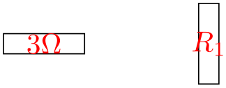
\node [resistor,point up,info=center:$R_1$] at
(2,0) {};
\end{tikzpicture}
-
/tikz/info'=[⟨options⟩]⟨angle⟩:⟨text⟩(no default) 
This key works exactly like the info key, only in case the ⟨angle⟩ is missing, it defaults to below instead of the current value of label position, which is usually above. This means that when you use info, you get a label above the node, while when you use the info' key you get a label below the node. In case the node has been rotated, the positions of the info nodes are rotated accordingly.
\usetikzlibrary {circuits.ee.IEC}
\begin{tikzpicture}[circuit ee IEC,every info/.style=red]
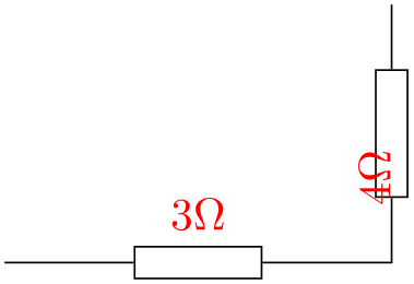
\draw (0,0) to[resistor={info={$3\Omega$},info'={$R_1$}}] (3,0)
to[resistor={info={$4\Omega$},info'={$R_2$}}] (3,2);
\end{tikzpicture}
-
/tikz/info sloped=[⟨options⟩]⟨angle⟩:⟨text⟩(no default) 
This key works like info, only the transform shape option is set when the label is drawn, causing it to follow the sloping of the main node.

\usetikzlibrary {circuits.ee.IEC}
\begin{tikzpicture}[circuit ee IEC,every info/.style=red]
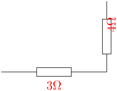
\draw (0,0) to[resistor={info sloped={$3\Omega$}}] (3,0)
to[resistor={info sloped={$4\Omega$}}] (3,2);
\end{tikzpicture}
-
/tikz/info' sloped=(no default) 
This is a combination of info' and info sloped.
                    \usetikzlibrary {circuits.ee.IEC}

                    \begin{tikzpicture}[circuit ee IEC,every info/.style=red]

                      \draw (0,0) to[resistor={info' sloped={$3\Omega$}}] (3,0)

                                  to[resistor={info' sloped={$4\Omega$}}] (3,2);

                    \end{tikzpicture}
-
/tikz/circuit declare unit={⟨name⟩}{⟨unit⟩}(no default) 
This key is used to declare keys that make it easy to attach physical units to nodes. The idea is that instead of info=$3\Omega$ you can write ohm=3 or instead of info'=$5\mathrm{S}$ you can write siemens'=5.
In detail, four keys are defined, namely /tikz/⟨name⟩, /tikz/⟨name⟩', /tikz/⟨name⟩ sloped, and /tikz/⟨name⟩' sloped. The arguments of all of these keys are of the form [⟨options⟩]⟨angle⟩:⟨value⟩ and it is passed (slightly modified) to the corresponding key info, info', info sloped, or info' sloped. The “slight modification” is the following: The text that is passed to the, say, info key is not ⟨value⟩, but rather $\mathrm{⟨value⟩⟨unit⟩}$
This means that after you said circuit declare unit={ohm}{\Omega}, then ohm=5k will have the same effect as info={[every ohm]$\mathrm{5k\Omega}$}. Here, every ohm is a style that allows you to configure the appearance of this unit. Since the info key is used internally, by changing the every info style, you can change the appearance of all units infos.
                    \usetikzlibrary {circuits.ee.IEC}

                    \begin{tikzpicture}[circuit ee IEC,circuit declare unit={my ohm}{O}]

                      \draw (0,0) to[resistor={my ohm' sloped=3}] (3,2);

                    \end{tikzpicture}
49.2.5 Declaring and Using Annotations
Annotations are quite similar to info labels. The main difference is that they generally cause something to be drawn by default rather than some text to be added (although an annotation might also add some text).
Annotations can be declared using the following key:
-
/tikz/circuit declare annotation={⟨name⟩}{⟨distance⟩}{⟨path⟩}(no default) 
-
1. The style every ⟨name⟩ is executed.
-
2. The following style is executed and then arrows=->:
-
/tikz/annotation arrow(style, no value) 
This style should set the > key to some desirable arrow tip.
-
-
3. The coordinate system is shifted such that the origin is at the north anchor of the symbol. (For the ⟨name⟩' key the coordinate system is flipped and shifted such that the origin is at the south anchor of the symbol.)
-
4. The label distance is locally set to ⟨distance⟩.
-
5. The parameter options given to the ⟨name⟩ key are executed.
-
6. The ⟨path⟩ is executed.
This key is used to declare an annotation named ⟨name⟩. Once declared, it can be used as an argument of a symbol and will add the drawing in ⟨path⟩ to the symbol. In detail, the following happens:
The Main Keys. Two keys called ⟨name⟩ and ⟨name⟩' are defined. The second causes the annotation to be “mirrored and placed on the other side” of the symbol. Both of these keys may also take further keys as parameter like info keys. Whenever the ⟨name⟩ key is used, a local scope is opened and in this scope the following things are done:
Usage. What all of the above amounts to is best explained by an example. Suppose we wish to create an annotation that
looks like a little circular arrow (like
 ). We could then say:
                    \tikzset{circuit declare annotation=

                    {circular annotation}

                        {9pt}

                        {(0pt,8pt) arc
                      (-270:80:3.5pt)}
 }
We can then use it like this:

                    {\usetikzlibrary {circuits.ee.IEC}} pre

                    \tikz[circuit ee IEC]

                      \draw (0,0) to
                    [resistor={circular annotation}]   (3,0);
Well, not very impressive since we do not see anything. This is due to the fact that the ⟨path⟩ becomes part of a path that contains the symbol node an nothing else. This path is not drawn or filled, so we do not see anything. What we must do is to use an edge path operation:

                    \usetikzlibrary {circuits.ee.IEC}

                    \tikzset{circuit declare annotation={circular annotation}{9pt}

                        {(0pt,8pt) edge[to path={arc(-270:80:3.5pt)}] ()}
 }

                    \tikz[circuit ee IEC]

                      \draw (0,0) to
                    [resistor={circular annotation}]   (3,0)

                                  to
                    [capacitor={circular annotation'}] (3,2);
The ⟨distance⟩ is important for the correct placement of additional info labels. When an annotation is present, the info labels may need to be moved further away from the symbol, but not always. For this reason, an annotation defines an additional ⟨distance⟩ that is applied to all info labels given as parameters to the annotation. Here is an example, that shows the difference:

                    {\usetikzlibrary {circuits.ee.IEC}} pre

                    \tikz[circuit ee IEC]

                      \draw (0,0) to
                    [resistor={circular
                      annotation,ohm=5}]   (2,0)

                                  to
                    [resistor={circular annotation={ohm=5}}] (4,0);
49.2.6 Theming Symbols
For each symbol, a certain graphical representation is chosen to actually show the symbol. You can modify this graphical representation in several ways:
-
• You can select a different library and use a different circuit ... key. This will change all graphics used for the symbols.
-
• You can generally change the size of graphic symbols by setting circuit size unit to a different value or using a key like small circuit symbols.
-
• You can add options to the graphics used by symbols either globally by setting the every circuit symbol style or locally by setting the every ⟨name⟩ style, where ⟨name⟩ is the name of a symbol. For instance, in the following picture the symbols are ridiculously thick and resistors are red.
                    \usetikzlibrary {circuits.ee.IEC}

                    \begin{tikzpicture}

                      [circuit ee IEC,

                       every circuit symbol/.style={ultra thick},

                       every resistor/.style={red}]


                      \draw (0,0) to
                    [inductor] ++(right:3) to
                    [resistor] ++(up:2);

                    \end{tikzpicture}
-
• You can selectively change the graphic used for a symbol by saying set resistor graphic=.
-
• You can change one or more of the following styles:
-
/tikz/circuit symbol open(style, initially draw) 
This style is used with symbols that consist of lines that surround some area. For instance, the IEC version of a resistor is an open symbol.
-
/tikz/circuit symbol filled(style, initially draw,fill=black) 
This style is used with symbols that are completely filled. For instance, the variant IEC version of an inductor is a filled, black rectangle.
-
/tikz/circuit symbol lines(style, initially draw) 
This style is used with symbols that consist only of lines that do not surround anything. Examples are a capacitor.
-
/tikz/circuit symbol wires(style, initially draw) 
This style is used for symbols that consist only of “wires”. The difference to the previous style is that a symbol consisting of wires will look strange when the lines are thicker than the lines of normal wires, while for symbols consisting of lines (but not wires) it may look nice to make them thicker. An example is the make contact symbol.
Compare
                        \usetikzlibrary {circuits.ee.IEC}

                        \tikz [circuit ee IEC,circuit symbol lines/.style={draw,very thick}]

                          \draw (0,0) to
                        [capacitor={near start},

                                          make contact={near end}] (3,0);
to

                        \usetikzlibrary {circuits.ee.IEC}

                        \tikz [circuit ee IEC,circuit symbol wires/.style={draw,very thick}]

                          \draw (0,0) to
                        [capacitor={near start},

                                          make contact={near end}] (3,0);
-
All circuit environments like circuit logic IEC mainly use options like set and gate graphic=... to set up the graphics used for a certain symbol. It turns out that graphic hidden in the “...” part is also always available as a separate style, whose name contains the library’s initials. For instance, the circuit logic IEC option actually contains the following command:
The and gate IEC graphic style, in turn, is defined as follows:
                \tikzset{and gate IEC graphic/.style=

                {

                    circuit symbol open,

                    circuit symbol size=width 2.5 height 4,

                    shape=and gate IEC,

                    inner sep=.5ex

                    }
 }
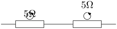
Normally, you do not need to worry about this, since you will not need to access a style like and gate IEC graphic directly; you will only use the and gate key. However, sometimes libraries define variants of a graphic; for instance, there are two variants for the resistor graphic in the IEC library. In this case you can set the graphic for the resistor to this variant (or back to the original) by saying set resistor graphic yourself:

                \usetikzlibrary {circuits.ee.IEC}

                \begin{tikzpicture}[circuit ee IEC]

                  % Standard resistor

                  \draw (0,2) to
                [resistor] (3,2);


                  % Var resistor

                  \begin{scope}[set resistor graphic=var resistor IEC graphic]

                    \draw (0,1) to
                [resistor] (3,1);


                    % Back to original

                    \draw [set resistor graphic=resistor IEC graphic]

                      (0,0) to
                [resistor] (3,0);

                  \end{scope}

                \end{tikzpicture}
49.3 Logical Circuits
49.3.1 Overview
A logical circuit is a circuit that contains what we call logical gates like an and gate or an xor gate. The logical libraries are intended to make it easy to draw such circuits.
In the following, we first have a look at the different libraries that can be used in principle and how the symbols look like. Then we have a more detailed look at how the symbols are used. Finally, we discuss the implementation details.
There are different ways of depicting logical gates, which is why there are different (sub-)libraries for drawing them. They provide the necessary graphical representations of the symbols declared in the following library:
-
TikZ Library circuits.logic 
\usetikzlibrary{circuits.logic} %
LaTeX
and plain
TeX
\usetikzlibrary[circuits.logic] % ConTeXt
This library declares the logical gate symbols, but does not provide the symbol graphics. The library also defines the
following key which, however, is also only used indirectly, namely by other libraries:
Since the circuits.logic library does not define any actual graphics, you need to use one of the following libraries, instead:
-
TikZ Library circuits.logic.IEC 
-
/tikz/circuit logic IEC(no value) 
\usetikzlibrary{circuits.logic.IEC} %
LaTeX
and plain
TeX
\usetikzlibrary[circuits.logic.IEC] % ConTeXt
This library provides graphics based on gates recommended by the International Electrotechnical Commission. When you include
this library, you can use the following key to set up a scope that contains a logical circuit where the gates are shown in
this style.
This key calls circuit logic and installs the IEC-like graphics for the logical symbols like and gate.
As explained in Section 49.2.6, for each graphic symbol of the library there is also a style that stores this particular appearance. These keys are called and gate IEC graphic, or gate IEC graphic, and so on.
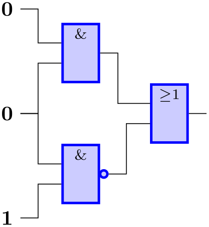
                        \usetikzlibrary {circuits.logic.IEC}

                        \begin{tikzpicture}[circuit logic IEC,

                                            every circuit symbol/.style={

                                              logic gate IEC symbol color=black,

                                              fill=blue!20,draw=blue,very thick}]

                          \matrix[column sep=7mm]

                          {

                            \node (i0) {0}; &
                                                   &
                        \\

                                            &
                        \node [and gate] (a1) {};  &
                        \\

                            \node (i1) {0}; &
                                                   &
                        \node [or gate] (o) {};\\

                                            &
                        \node [nand gate] (a2) {}; &
                        \\

                            \node (i2) {1}; &
                                                   &
                        \\

                          };

                          \draw (i0.east) --
                        ++(right:3mm) |-
                        (a1.input 1);

                          \draw (i1.east) --
                        ++(right:3mm) |-
                        (a1.input 2);

                          \draw (i1.east) --
                        ++(right:3mm) |-
                        (a2.input 1);

                          \draw (i2.east) --
                        ++(right:3mm) |-
                        (a2.input 2);

                          \draw (a1.output) --
                        ++(right:3mm) |-
                        (o.input 1);

                          \draw (a2.output) --
                        ++(right:3mm) |-
                        (o.input 2);

                          \draw (o.output) --
                        ++(right:3mm);

                        \end{tikzpicture}
-
TikZ Library circuits.logic.US 
-
/tikz/circuit logic US(no value) 
\usetikzlibrary{circuits.logic.US} %
LaTeX
and plain
TeX
\usetikzlibrary[circuits.logic.US] % ConTeXt
This library provides graphics showing “American” logic gates. It defines the following key:
This style calls circuit logic and installs US-like graphics for the logical symbols like and gate. For instance, it says
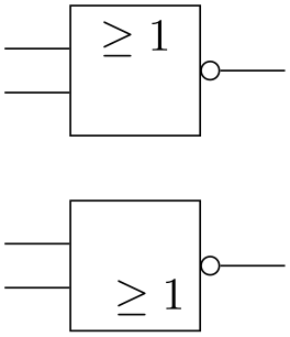
Here is an example:
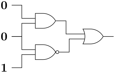
                        \usetikzlibrary {circuits.logic.CDH}

                        \begin{tikzpicture}[circuit logic CDH,

                                            tiny circuit symbols,

                                            every circuit symbol/.style={

                                              fill=white,draw}]

                          \matrix[column sep=7mm]

                          {

                            \node (i0) {0}; &
                                                   &
                        \\

                                            &
                        \node [and gate] (a1) {};  &
                        \\

                            \node (i1) {0}; &
                                                   &
                        \node [or gate] (o) {};\\

                                            &
                        \node [nand gate] (a2) {}; &
                        \\

                            \node (i2) {1}; &
                                                   &
                        \\

                          };

                          \draw (i0.east) --
                        ++(right:3mm) |-
                        (a1.input 1);

                          \draw (i1.east) --
                        ++(right:3mm) |-
                        (a1.input 2);

                          \draw (i1.east) --
                        ++(right:3mm) |-
                        (a2.input 1);

                          \draw (i2.east) --
                        ++(right:3mm) |-
                        (a2.input 2);

                          \draw (a1.output) --
                        ++(right:3mm) |-
                        (o.input 1);

                          \draw (a2.output) --
                        ++(right:3mm) |-
                        (o.input 2);

                          \draw (o.output) --
                        ++(right:3mm);

                        \end{tikzpicture}
-
TikZ Library circuits.logic.CDH 
-
/tikz/circuit logic CDH(no value) 
\usetikzlibrary{circuits.logic.CDH} %
LaTeX
and plain
TeX
\usetikzlibrary[circuits.logic.CDH] % ConTeXt
This library provides graphics based on the logic symbols used in A. Croft, R. Davidson, and M. Hargreaves (1992),
Engineering Mathematics, Addison-Wesley, 82–95. They are identical to the US-style symbols, except for the
and- and nand-gates.
This key calls circuit logic US and installs the two special and- and nand-gates, that is, it uses set and gate graphic with and gate CDH graphic and likewise for nand-gates.
Inside circuit logic XYZ scopes, you can now use the keys shown in Section 49.3.2. We have a more detailed look at one of them, all the other work the same way:
-
/tikz/and gate(no value) 
-
/tikz/inputs=⟨input list⟩ (no default, initially {normal,normal})
This key should be passed to a node command. It will cause the node to “look like” an and gate, where the exact appearance of the gate is dictated by the which circuit environment is used. To further configure the appearance of the and gate, see Section 49.2.6.
                    \usetikzlibrary {circuits.logic.IEC}

                    \tikz [circuit logic IEC] \node [and gate] {$A$};

                    \usetikzlibrary {circuits.logic.US}

                    \tikz [circuit logic US]

                    {

                      \node [and gate,point down] {$A$};

                      \node [and gate,point down,info=center:$A$] at
                    (1,0) {};

                    }
Inputs. Multiple inputs can be specified for a logic gate (provided they support multiple inputs: a not gate – also known as an inverter – does not). However, there is an upper limit for the number of inputs which has been set to 1024, which should be way more than would ever be needed.
The following key is used to configure the inputs. It is available only inside a circuit logic environment.
If a gate has \(n\) inputs, the ⟨input list⟩ should consists of \(n\) letters, each being i for “inverted” or n for “normal”. Inverted gates will be indicated by a little circle. In any case the anchors for the inputs will be set up appropriately, numbered from top to bottom input 1, input 2, …and so on. If the gate only supports one input the anchor is simply called input with no numerical index.

                        \usetikzlibrary {circuits.logic.IEC}

                        \begin{tikzpicture}[circuit logic IEC]

                          \node[and gate,inputs={inini}] (A) {};

                          \foreach \a in
                        {1,...,5}

                            \draw (A.input \a -| -1,0) --
                        (A.input \a);

                          \draw (A.output) --
                        ++(right:5mm);

                        \end{tikzpicture}
(This key is just a shorthand for logic gate inputs, described in detail in section 49.3.3. There you will also find descriptions of how to configure the size of the inverted circles and the way the symbol size increases when there are too many inputs.)
Output. Every logic gate has one anchor called output.
49.3.2 Symbols: The Gates
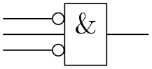
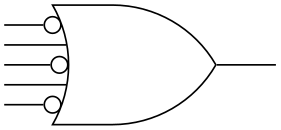
The following table shows which symbols are declared by the main circuits.logic library and their appearance in the different sublibraries.
| Key | Appearance inside | Appearance inside | Appearance inside |
| circuit logic IEC | circuit logic US | circuit logic CDH | |
| /tikz/and gate |
|

|

|
| /tikz/nand gate |

|

|

|
| /tikz/or gate |

|

|

|
| /tikz/nor gate |

|

|

|
| /tikz/xor gate |

|

|

|
| /tikz/xnor gate |

|

|

|
| /tikz/not gate |

|

|

|
| /tikz/buffer gate |

|

|

|
49.3.3 Implementation: The Logic Gates Shape Library
The previous sections described the TikZ interface for creating logical circuits. In this section we take a closer look at the underlying pgf libraries.
Just as there are several TikZ circuit libraries, there are two underlying pgf shape libraries, one for creating US-style gates and one for IEC-style gates. These libraries define shapes only. It is the job of the circuit libraries to “theme” them so that they “look nice”. However, in principle, you can also use these shapes directly.
Let us begin with the base library that defines the handling of inputs.
-
TikZ Library shapes.gates.logic 
-
/pgf/logic gate inputs=⟨input list⟩ (no default, initially {normal,normal}) 
-
/pgf/logic gate inverted radius=⟨length⟩ (no default, initially 2pt) 
-
/pgf/logic gate input sep=⟨length⟩ (no default, initially .125cm) 
\usepgflibrary{shapes.gates.logic} %
LaTeX
and plain
TeX
and pure pgf
\usepgflibrary[shapes.gates.logic] % ConTeXt and pure pgf
\usetikzlibrary{shapes.gates.logic} %
LaTeX
and plain
TeX
when using TikZ
\usetikzlibrary[shapes.gates.logic] % ConTeXt when using TikZ
This library defines common keys used by all logical gate shapes.
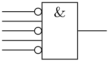
Specify the inputs for the logic gate. The keyword inverted indicates an inverted input which will mean pgf will draw a circle attached to the main shape of the logic gate. Any keyword that is not inverted will be treated as a “normal” or “non-inverted” input (however, for readability, you may wish to use normal or non-inverted), and pgf will not draw the circle. In both cases the anchors for the inputs will be set up appropriately, numbered from top to bottom input 1, input 2, …and so on. If the gate only supports one input the anchor is simply called input with no numerical index.

                        \usetikzlibrary {circuits.logic.IEC}

                        \begin{tikzpicture}[minimum height=0.75cm]

                          \node[and gate IEC, draw, logic gate inputs={inverted, normal, inverted}]

                            (A) {};

                          \foreach \a in
                        {1,...,3}

                            \draw (A.input \a -| -1,0) --
                        (A.input \a);

                          \draw (A.output) --
                        ([xshift=0.5cm]A.output);

                        \end{tikzpicture}
For multiple inputs it may be somewhat unwieldy to specify a long list, thus, the following “shorthand” is permitted (this is an extension of ideas due to Jürgen Werber and Christoph Bartoschek): Using i for inverted and n for normal inputs, ⟨input list⟩ can be specified without the commas. So, for example, ini is equivalent to inverted, normal, inverted.
                        \usetikzlibrary {circuits.logic.US}

                        \begin{tikzpicture}[minimum height=0.75cm]

                          \node[or gate US, draw,logic gate inputs=inini] (A) {};

                          \foreach \a in
                        {1,...,5}

                            \draw (A.input \a -| -1,0) --
                        (A.input \a);

                          \draw (A.output) --
                        ([xshift=0.5cm]A.output);

                        \end{tikzpicture}
The height of the gate may be increased to accommodate the number of inputs. In fact, it depends on three variables: \(n\), the number of inputs, \(r\), the radius of the circle used to indicate an inverted input and \(s\), the distance between the centers of the inputs. The default height is then calculated according to the expression \((n+1)\times \max (2r,s)\). This then may be increased to accommodate the node contents or any minimum size specifications.
The radius of the inverted input circle and the distance between the centers of the inputs can be customized using the following keys:
Set the radius of the circle that is used to indicate inverted inputs. This is also the radius of the circle used for the inverted output of the nand, nor, xnor and not gates.
                        \usetikzlibrary {circuits.logic.CDH}

                        \begin{tikzpicture}[minimum height=0.75cm]

                          \tikzset{every node/.style={shape=nand gate CDH, draw, logic gate inputs=ii}}

                          \node[logic gate inverted radius=2pt] {A};

                          \node[logic gate inverted radius=4pt] at
                        (0,-1) {B};

                        \end{tikzpicture}
Set the distance between the centers of the inputs to the logic gate.

                        \usetikzlibrary {circuits.logic.IEC}

                        \begin{tikzpicture}[minimum size=0.75cm]

                          \draw [help lines] grid
                        (3,2);

                          \tikzset{every node/.style={shape=and gate IEC, draw, logic gate inputs=ini}}

                          \node[logic gate input sep=0.33333cm] at
                        (1,1)(A) {A};

                          \node[logic gate input sep=0.5cm]     at
                        (3,1) (B) {B};

                          \foreach \a in
                        {1,...,3}

                            \draw (A.input \a -| 0,0) --
                        (A.input \a)

                                  (B.input \a -| 2,0) --
                        (B.input \a);

                        \end{tikzpicture}
pgf will increase the size of the logic gate to accommodate the number of inputs, and the size of the inverted radius and the separation between the inputs. However with all shapes in this library, any increase in size (including any minimum size requirements) will be applied so that the default aspect ratio is unaltered. This means that changing the height will change the width and vice versa.
49.3.4 Implementation: The US-Style Logic Gates Shape Library
-
TikZ Library shapes.gates.logic.US 
-
/pgf/logic gate anchors use bounding box=⟨boolean⟩ (no default, initially false) 
-
• and gate US, two or more inputs
-
• and gate CDH, two or more inputs
-
• nand gate US, two or more inputs
-
• nand gate CDH, two or more inputs
-
• or gate US, two or more inputs
-
• nor gate US, two or more inputs
-
• xor gate US, two or more inputs
-
• xnor gate US, two or more inputs
-
• not gate US, one input
-
• buffer gate US, one input
-
Shape nand gate US 
\usepgflibrary{shapes.gates.logic.US} %
LaTeX
and plain
TeX
and pure pgf
\usepgflibrary[shapes.gates.logic.US] % ConTeXt and pure pgf
\usetikzlibrary{shapes.gates.logic.US} %
LaTeX
and plain
TeX
when using TikZ
\usetikzlibrary[shapes.gates.logic.US] % ConTeXt when using TikZ
This library provides “American” logic gate shapes whose names are suffixed with the identifier
US. Additionally, alternative and and
nand gates are provided which are based on the logic symbols used in A. Croft, R. Davidson, and M.
Hargreaves (1992), Engineering Mathematics, Addison-Wesley, 82–95. These two shapes are suffixed with
CDH.
The “compass point” anchors apply to the main part of the shape and do not include any inverted inputs or outputs. This library provides an additional feature to facilitate the relative positioning of logic gates:
When set to true this key will ensure that the compass point anchors use the bounding rectangle of the main shape, which, ignore any inverted inputs or outputs, but includes any outer sep. This only affects the compass point anchors and is not set on a shape by shape basis: whether the bounding box is used is determined by value of this key when the anchor is accessed.
                        \usetikzlibrary {circuits.logic.US}

                        \begin{tikzpicture}[minimum height=1.5cm]

                          \node[xnor gate US, draw, gray!50,line width=2pt] (A) {};

                          \foreach \x/\y/\z in
                        {false/blue/1pt, true/red/2pt}

                            \foreach \a in
                        {north, south, east, west, north
                        east,

                              south
                        east, north
                        west, south
                        west}

                              \draw[logic gate anchors use bounding box=\x, color=\y]

                                (A.\a) circle(\z);

                        \end{tikzpicture}
The library defines a number of shapes. For each shape the allowed number of inputs is also shown:
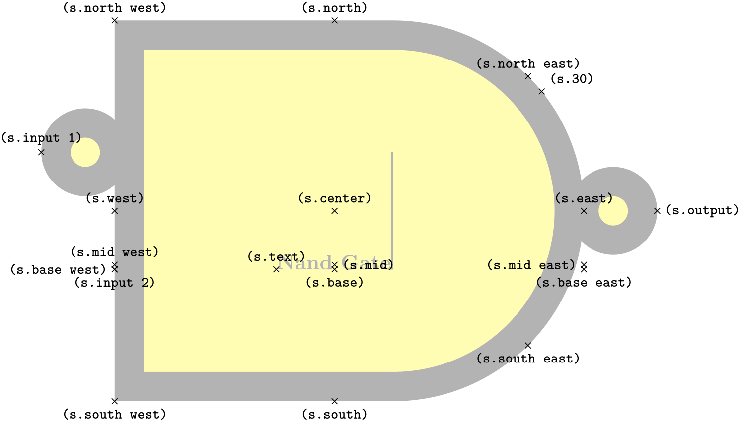
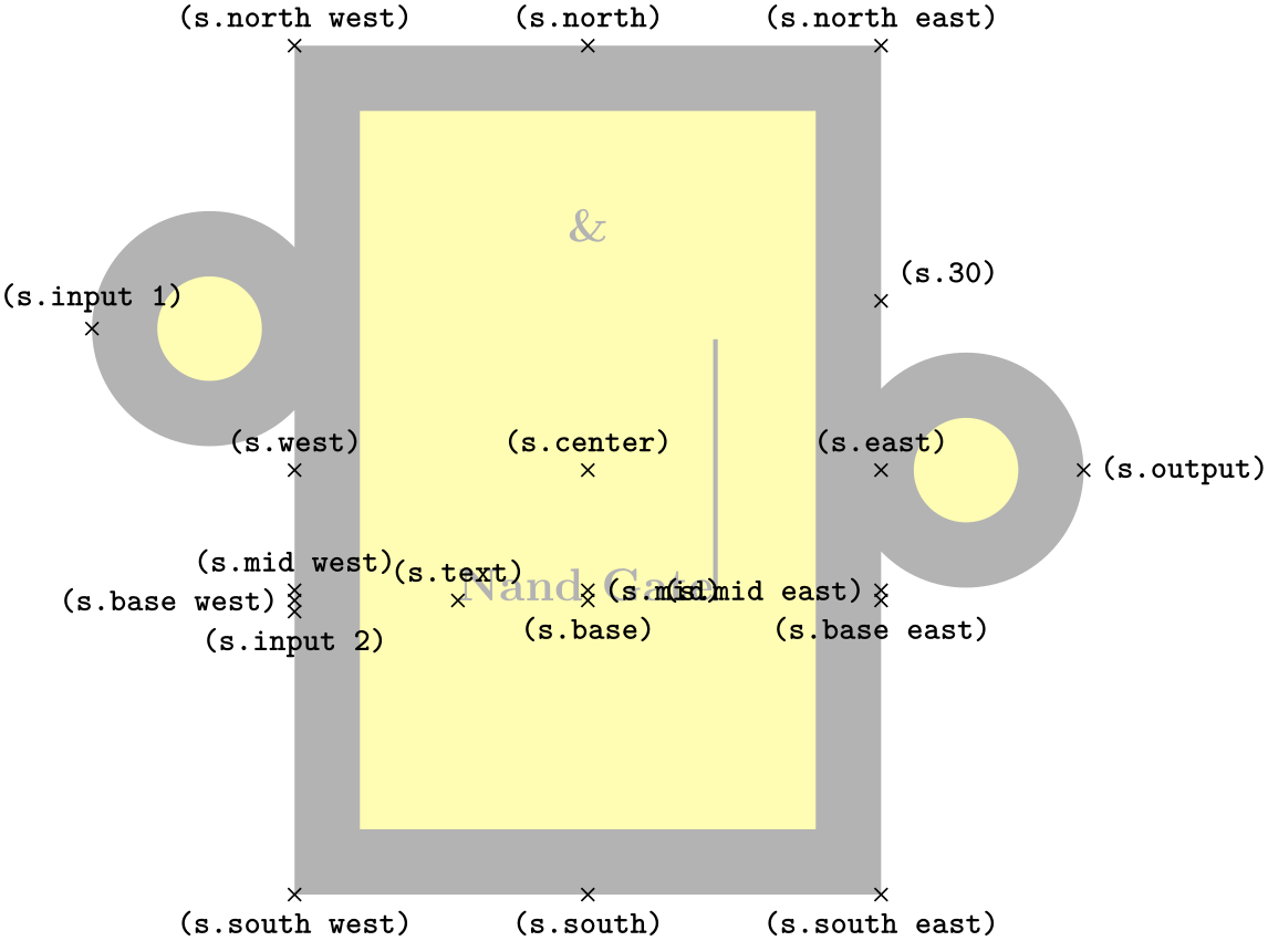
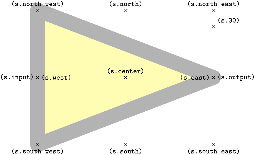
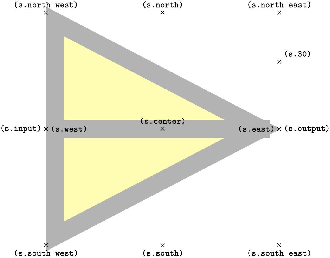
In the following, we only have a detailed look at the anchors defined by one of them. We choose the nand gate US because it shows all the “interesting” anchors.
This shape is a nand gate, which supports two or more inputs. If less than two inputs are specified an error will result. The anchors for this gate with two non-inverted inputs (using the normal compass point anchors) are shown below. Anchor 30 is an example of a border anchor.
                        \usetikzlibrary {circuits.logic.US}

                        \Huge

                        \begin{tikzpicture}

                          \node[name=s,shape=nand gate US,shape example, inner sep=0cm,

                          logic gate inputs={in},

                          logic gate inverted radius=.5cm] {Nand
                        Gate\vrule width1pt
                        height2cm};

                          \foreach \anchor/\placement in

                            {center/above, text/above, 30/above
                        right,

                             mid/right, mid
                        east/left, mid
                        west/above,

                             base/below, base
                        east/below, base
                        west/left,

                             north/above, south/below, east/above, west/above,

                             north
                        east/above, south
                        east/below, south
                        west/below, north
                        west/above,

                             output/right, input
                        1/above, input
                        2/below}

                             \draw[shift=(s.\anchor)] plot[mark=x] coordinates{(0,0)}

                               node[\placement] {\scriptsize\texttt{(s.\anchor)}};

                        \end{tikzpicture}
(For the definition of the shape example style, see Section 71.)
49.3.5 Implementation: The IEC-Style Logic Gates Shape Library
-
TikZ Library shapes.gates.logic.IEC 
-
/pgf/and gate IEC symbol=⟨text⟩ (no default, initially \char`\&) 
-
/pgf/nand gate IEC symbol=⟨text⟩ (no default, initially \char`\&) 
-
/pgf/or gate IEC symbol=⟨text⟩ (no default, initially $\geq1$) 
-
/pgf/nor gate IEC symbol=⟨text⟩ (no default, initially $\geq1$) 
-
/pgf/xor gate IEC symbol=⟨text⟩ (no default, initially {$=1$}) 
-
/pgf/xnor gate IEC symbol=⟨text⟩ (no default, initially {$=1$}) 
-
/pgf/not gate IEC symbol=⟨text⟩ (no default, initially 1) 
-
/pgf/buffer gate IEC symbol=⟨text⟩ (no default, initially 1) 
-
/pgf/logic gate IEC symbol align=⟨align⟩ (no default, initially top) 
-
/pgf/logic gate IEC symbol color=⟨color⟩(no default) 
-
• and gate IEC, two or more inputs
-
• nand gate IEC, two or more inputs
-
• or gate IEC, two or more inputs
-
• nor gate IEC, two or more inputs
-
• xor gate IEC, two or more inputs
-
• xnor gate IEC, two or more inputs
-
• not gate IEC, one input
-
• buffer gate IEC, one input
-
Shape nand gate IEC 
\usepgflibrary{shapes.gates.logic.IEC} %
LaTeX
and plain
TeX
and pure pgf
\usepgflibrary[shapes.gates.logic.IEC] % ConTeXt and pure pgf
\usetikzlibrary{shapes.gates.logic.IEC} %
LaTeX
and plain
TeX
when using TikZ
\usetikzlibrary[shapes.gates.logic.IEC] % ConTeXt when using TikZ
This library provides rectangular logic gate shapes. These shapes are suffixed with IEC as they
are based on gates recommended by the International Electrotechnical Commission.
By default each gate is drawn with a symbol, \(\texttt {\&}\) for and and nand gates, \(\geq 1\) for or and nor gates, \(1\) for not and buffer gates, and \(=1\) for xor and xnor gates. These symbols are drawn automatically (internally they are drawn using the “foreground” path), and are not strictly speaking part of the node contents. However, the gate is enlarged to make sure the symbols are within the border of the node. It is possible to change the symbols and their position within the node using the following keys:
Set the symbol for the and gate. Note that if the node is filled, this color will be used for the symbol, making it invisible, so it will be necessary set ⟨text⟩ to something like \color{black}\char`\&. Alternatively, the logic gate IEC symbol color key can be used to set the color of all symbols simultaneously.
In TikZ, when the use IEC style logic gates key has been used, this key can be replaced by and gate symbol.
Set the symbol for the nand gate. In TikZ, when the use IEC style logic gates key has been used, this key can be replaced by nand gate symbol.
Set the symbol for the or gate. In TikZ, when the use IEC style logic gates key has been used, this key can be replaced by or gate symbol.
Set the symbol for the nor gate. In TikZ, when the use IEC style logic gates key has been used, this key can be replaced by nor gate symbol.
Set the symbol for the xor gate. Note the necessity for braces, as the symbol contains =. In TikZ, when the use IEC style logic gates key has been used, this key can be replaced by xor gate symbol.
Set the symbol for the xnor gate. In TikZ, when the use IEC style logic gates key has been used, this key can be replaced by xnor gate symbol.
Set the symbol for the not gate. In TikZ, when the use IEC style logic gates key has been used, this key can be replaced by not gate symbol.
Set the symbol for the buffer gate. In TikZ, when the use IEC style logic gates key has been used, this key can be replaced by buffer gate symbol.
Set the alignment of the logic gate symbol (in TikZ, when the use IEC style logic gates key has been used, IEC can be omitted). The specification in ⟨align⟩ is a comma separated list from top, bottom, left or right. The distance between the border of the node and the outer edge of the symbol is determined by the values of the inner xsep and inner ysep.
                        \usetikzlibrary {shapes.gates.logic.IEC}

                        \begin{tikzpicture}[minimum size=1cm, use IEC style logic gates]

                            \tikzset{every node/.style={nor gate, draw}}

                          \node (A) at
                        (0,1.5) {};

                          \node [logic gate symbol align={bottom, right}] (B) at
                        (0,0) {};

                          \foreach \g in
                        {A, B}{

                            \foreach \i in
                        {1,2}

                              \draw ([xshift=-0.5cm]\g.input \i) --
                        (\g.input \i);

                            \draw (\g.output) --
                        ([xshift=0.5cm]\g.output);

                          }

                        \end{tikzpicture}
This key sets the color for all symbols simultaneously. This color can be overridden on a case by case basis by specifying a color when setting the symbol text.
The library defines the following shapes:
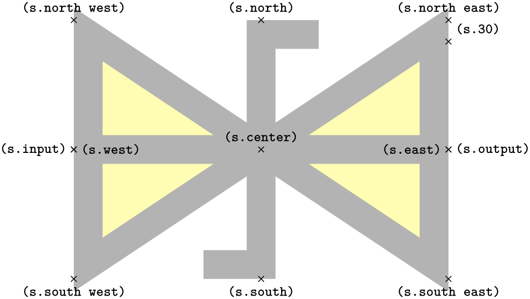
Again, we only have a look at the nand-gate in more detail:
This shape is a nand gate. It supports two or more inputs. If less than two inputs are specified an error will result. The anchors for this gate with two inverted inputs are shown below. Anchor 30 is an example of a border anchor.
                        \usetikzlibrary {circuits.logic.IEC}

                        \Huge

                        \begin{tikzpicture}

                          \node[name=s,shape=nand gate IEC ,shape example, inner xsep=1cm, inner ysep=1cm,

                            minimum height=6cm, nand gate IEC symbol=\color{black!30}\char`\&,

                            logic gate inputs={in},

                            logic gate inverted radius=0.65cm]

                          {Nand
                        Gate\vrule width1pt
                        height2cm};

                          \foreach \anchor/\placement in

                            {center/above, text/above, 30/above
                        right,

                             mid/right, mid
                        east/left, mid
                        west/above,

                             base/below, base
                        east/below, base
                        west/left,

                             north/above, south/below, east/above, west/above,

                             north
                        east/above, south
                        east/below, south
                        west/below, north
                        west/above,

                             output/right, input
                        1/above, input
                        2/below}

                             \draw[shift=(s.\anchor)] plot[mark=x] coordinates{(0,0)}

                               node[\placement] {\scriptsize\texttt{(s.\anchor)}};

                        \end{tikzpicture}
49.4 Electrical Engineering Circuits
49.4.1 Overview
An electrical engineering circuit contains symbols like resistors or capacitors or voltage sources and annotations like the two arrows pointing toward an element whose behaviour is light dependent. The electrical engineering libraries, abbreviated ee-libraries, provide such symbols and annotations.
Just as for logical gates, there are different ways of drawing ee-symbols. Currently, there is one main library for drawing circuits, which uses the graphics from the International Electrotechnical Commission, but you can add your own libs. This is why, just as for logical gates, there is a base library and more specific libraries.
-
TikZ Library circuits.ee 
\usetikzlibrary{circuits.ee} %
LaTeX
and plain
TeX
\usetikzlibrary[circuits.ee] % ConTeXt
This library declares the ee symbols, but (mostly) does not provide the symbol graphics, which is left to the sublibraries.
Just like the logical gates library, a key is defined that is normally only used internally:
The library also declares some standard annotations and units.
As for logical circuits, to draw a circuit the first step is to include a library containing the symbols graphics. Currently, you have to include circuits.ee.IEC.
-
TikZ Library circuits.ee.IEC 
-
/tikz/circuit ee IEC(no value) 
\usetikzlibrary{circuits.ee.IEC} %
LaTeX
and plain
TeX
\usetikzlibrary[circuits.ee.IEC] % ConTeXt
When this library is loaded, you can use the following style:
This style calls circuit ee and installs the IEC-like graphics for the logical symbols like resistor.
Inside the circuit ee IEC scope, you can now use the keys for symbols, units, and annotations listed in the later sections. We have a more detailed look at one of each of them, all the others work the same way.
Let us start with an example of a symbol: the resistor symbol. The other predefined symbols are listed in Section 49.4.2 and later sections.
-
/tikz/resistor=⟨options⟩(no default) 
-
1. The path currently being constructed is cut up to make place for a node.
-
2. This node will be a resistor node that is rotated so that it points “along” the path (unless an option like shift only or an extra rotation is used to change this).
-
3. The ⟨options⟩ passed to the resistor key are passed on to the node.
-
4. The ⟨options⟩ are pre-parsed to identify a pos key or a key like at start or midway. These keys are used to determine where on the to path the node will lie.
This key should be used with a node path command or with the to path command.
Using the Key with Normal Nodes. When used with a node, it will cause this node to “look like” a resistor (by default, in the IEC library, this is just a simple rectangle).
                    \usetikzlibrary {circuits.ee.IEC}

                    \tikz [circuit ee IEC]

                      \node [resistor] {};
Unlike normal nodes, a resistor node generally should not take any text (as in node [resistor] {foo}). Instead, the labeling of resistors should be done using the label, info and ohm options.

                    \usetikzlibrary {circuits.ee.IEC}

                    \tikz [circuit ee IEC]

                      \node [resistor,ohm=5] {};
The ⟨options⟩ make no real sense when the resistor option is used with a normal node, you can just as well given them to the node itself. Thus, the following has the same effect as the above example:

                    \usetikzlibrary {circuits.ee.IEC}

                    \tikz [circuit ee IEC]

                      \node [resistor={ohm=5}] {};
In a circuit, you will often wish to rotate elements. For this, the options point up, point down, point left or point right may be especially useful. They are just shorthands for appropriate rotations like rotate=90.
Using the Key on a To Path. When the resistor key is used on a to path inside a circuit ee IEC, the circuit handle symbol key is called internally. This has a whole bunch of effects:
Since the ⟨options⟩ of the resistor key are passed on to the resistor node on the path, you can use it to add labels to the node. Here is a simple example:
You can add multiple labels to a resistor and you can have multiple resistors (or other elements) on a single path.
Inputs, Outputs, and Anchors. Like the logical gates, all ee-symbols have an input and an output anchor. Special-purpose-nodes may have even more anchors of this type. Furthermore, the ee-symbols-nodes also have four standard compass direction anchors.
Changing the Appearance. To configure the appearance of all resistors, see Section 49.2.6. You can use the ⟨options⟩ to locally change the appearance of a single resistor.
Let us now have a look at an example of a unit: the Ohm unit. The other predefined units are listed in Section 49.4.7.
-
/tikz/ohm=⟨value⟩(no default) 
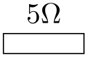
This key is used to add an info label to a node with a special text: $\mathrm{⟨value⟩\Omega}$. In other words, the ohm key can only be used with the options of a node and, when used, it will cause the ⟨value⟩ to be placed next to the node, followed by \(\Omega \). Since the ⟨value⟩ is typeset inside a \mathrm command, when you write ohm=5k you get \(\mathrm {5k\Omega }\), ohm=5p yields \(\mathrm {5p\Omega }\), and ohm=5.6\cdot 10^{2}\mu yields \(\mathrm {5.6\cdot 10^{2}\mu \Omega }\).
                    \usetikzlibrary {circuits.ee.IEC}

                    \tikz [circuit ee IEC] \draw (0,0) to
                    [resistor={ohm=5M}] (0,2);
Instead of ohm you can also use ohm', which places the label on the other side.

                    \usetikzlibrary {circuits.ee.IEC}

                    \tikz [circuit ee IEC] \draw (0,0) to
                    [resistor={ohm'=5M}] (0,2);
Finally, there are also keys ohm sloped and ohm' sloped for having the info label rotate together with the main node.

You can configure the appearance of an Ohm info label using the key every ohm.
Finally, let us have a look at an annotation: the light emitting annotation. The other predefined units are listed in Section 49.4.8.
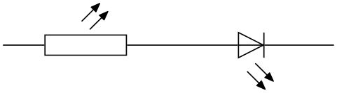
-
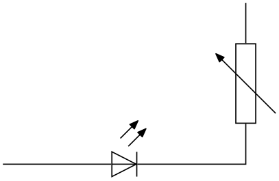
/tikz/light emitting=⟨options⟩(no default) 
-
1. You can use keys like red to change the appearance of this annotation, locally.
-
2. You can use keys like <- or -latex to change the direction and kinds of arrows used in the annotation.
-
3. You can use info labels like ohm=5 or info=foo inside the ⟨options⟩. These info labels will be added to the main node (not to the annotation itself), but the label distance will have been changed to accommodate for the space taken up by the annotation.

-
• You can set the every circuit annotation style.
-
• You can set the every light emitting style.
-
• You can set the following key:
-
/tikz/annotation arrow(style, no value)
This style should set the default > arrow to some nice value.
-
Like a unit, an annotation should be given as an additional option to a node. It causes some drawings (in this case, two parallel lines) to be placed next to the node.
                    \usetikzlibrary {circuits.ee.IEC}

                    \tikz [circuit ee IEC] \draw (0,0) to
                    [diode=light emitting] (2,0);
The ⟨options⟩ can be used for three different things:
In addition to light emitting there is also a key called light emitting', which simply places the annotation on the other side of the node.
You can configure the appearance of annotations in three ways:
49.4.2 Symbols: Indicating Current Directions
There are two symbols for indicating current directions. These symbols are defined directly inside circuit ee.
|
Key |
Appearance | |

|
||

|
The examples have been produced by (in essence) \draw (0,0) to[⟨symbol name⟩] (3,0);.
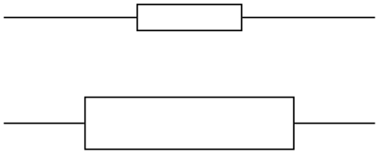
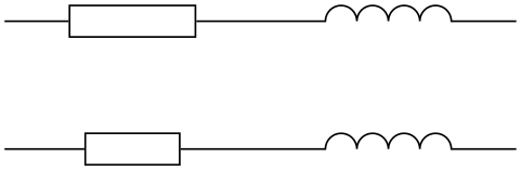
49.4.3 Symbols: Basic Elements
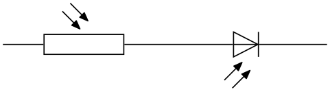
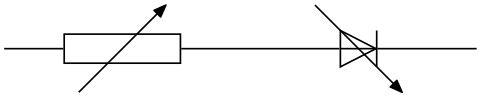
The following table show basic symbols as they are depicted inside the circuit ee IEC environment. To install one of alternate graphics, you have to say set ⟨symbol name⟩ graphic=var ⟨symbol name⟩ IEC graphic.
|
Key |
Appearance | Alternate appearance |
|
/tikz/resistor |

|

|

|

|
|
|
/tikz/capacitor |

|
|
|
/tikz/battery |

|
|
|
/tikz/bulb |

|
|
|
/tikz/current source |

|
|
|
/tikz/voltage source |

|
|
|
/tikz/ac source |

|
|
|
/tikz/dc source |

|
|
|
/tikz/ground |

|
49.4.4 Symbols: Diodes
The following table shows diodes as they are depicted inside the circuit ee IEC environment.
|
Key |
Appearance | Alternate appearance |

|

|
|

|

|
|
|
/tikz/Schottky diode |

|

|
|
/tikz/tunnel diode |

|

|
|
/tikz/backward diode |

|

|
|
/tikz/breakdown diode |

|

|
49.4.5 Symbols: Contacts
The following table shows contacts as they are depicted inside the circuit ee IEC environment.
|
Key |
Appearance | Alternate appearance |

|
||

|

|
|
|
/tikz/break contact |

|
49.4.6 Symbols: Measurement devices
The following table shows measurement devices as they are depicted inside the circuit ee IEC environment.
|
Key |
Appearance | |

|
||

|
||
|
/tikz/ohmmeter |

|
49.4.7 Units
The circuits.ee library predefines the following unit keys:
|
Key |
Appearance of \(1\) unit |

|
|

|
|
|
/tikz/ohm |

|
|
/tikz/siemens |

|
|
/tikz/henry |

|
|
/tikz/farad |

|
|
/tikz/coulomb |

|
|
/tikz/voltampere |

|
|
/tikz/watt |

|
|
/tikz/hertz |

|
49.4.8 Annotations
The circuits.ee.IEC library defines the following annotations:
|
Key |
Appearance | |
|
/tikz/light emitting |

|
|
|
||
|
/tikz/direction info |
|
|
|
/tikz/adjustable |

|
The lines have been produced using, in essence,
and similarly for the other annotations.
49.4.9 Implementation: The EE-Symbols Shape Library
The TikZ libraries depend on two shape libraries, which are included automatically. Usually, you will not need to use these shapes directly.
-
TikZ Library shapes.gates.ee 
-
• rectangle ee
-
• circle ee
-
• direction ee
\usepgflibrary{shapes.gates.ee} %
LaTeX
and plain
TeX
and pure pgf
\usepgflibrary[shapes.gates.ee] % ConTeXt and pure pgf
\usetikzlibrary{shapes.gates.ee} %
LaTeX
and plain
TeX
when using TikZ
\usetikzlibrary[shapes.gates.ee] % ConTeXt when using TikZ
This library defines basic shapes that can be used by all ee-circuit libraries. Currently, it defines the following shapes:
Additionally, the library defines the following arrow tip: The direction ee arrow tip is basically the same as a triangle 45 arrow tip with rounded joins.
| direction ee |
yields thick
 and thin

|
However, unlike normal arrow tips, its size does not depend on the current line width. Rather, it depends on the value of its arrow options, which should be set to the desired size. Thus, you should say something like \pgfsetarrowoptions{direction ee}{5pt} to set the size of the arrow.
-
Shape rectangle ee 
This shape is completely identical to a normal rectangle, only there are two additional anchors: The input anchor is an alias for the west anchor, while the output anchor is an alias for the east anchor.
-
Shape circle ee 
Like the rectangle ee shape, only for circles.
-
Shape direction ee 
-
/pgf/direction ee arrow=⟨right arrow tip name⟩(no default) 
-
1. The size of the shape is computed according to the following rules: The width of the shape is set up so that the left border of the shape is at the left end of the arrow tip and the right border is at the right end of the arrow tip. These left and right “ends” of the arrow are the tip end and the back end specified by the arrow itself (see Section 105.2 for details). You usually need not worry about this width setting.
By comparison, the height of the arrow is given by the current setting of minimum height. Thus, this key must have been set up correctly to reflect the “real” height of the arrow tip. The reason is that the height of an arrow is not specified when arrows are declared and is, thus, not available, here.
Possibly, the height computation will change in the future to reflect the real height of the arrow, so you should generally set up the minimum height to be the same as the real height.
-
2. A straight line from left to right inside the shape’s boundaries is added to the background path.
-
3. The arrow tip, pointing right, is drawn before the background path.
This shape is rather special. It is intended to be used to “turn an arrow tip into a shape”. First, you should set the following key to the name of an arrow tip:
The value of this key will be used for the arrow tip depicted in an direction ee shape.
When a node of shape direction ee is created, several things happen:
The anchors of this shape are just the compass anchors, which lie on a rectangle whose width and height are the above-computed height and width.

                    \usetikzlibrary {circuits.ee.IEC}

                    \begin{tikzpicture}

                      \pgfsetarrowoptions{direction
                    ee}{6cm}

                      \node[name=s,shape=direction ee,shape example,minimum height=0.7654*6cm] {};

                      \foreach \anchor/\placement in

                        {center/above, 30/above
                    right,

                         north/above, south/below, east/left, west/right,

                         north
                    east/above, south
                    east/below, south
                    west/below, north
                    west/above,

                         input/left,output/right}

                         \draw[shift=(s.\anchor)] plot[mark=x] coordinates{(0,0)}

                           node[\placement] {\scriptsize\texttt{(s.\anchor)}};

                    \end{tikzpicture}
                    \usetikzlibrary {circuits.ee.IEC}

                    \begin{tikzpicture}[direction ee arrow=angle 45]

                      \node[name=s,shape=direction ee,shape example,minimum height=1.75cm] {};

                      \foreach \anchor/\placement in
                    {north/above, south/below,

                                                      output/right, input/left}

                         \draw[shift=(s.\anchor)] plot[mark=x] coordinates{(0,0)}

                           node[\placement] {\scriptsize\texttt{(s.\anchor)}};

                    \end{tikzpicture}
49.4.10 Implementation: The IEC-Style EE-Symbols Shape Library
-
TikZ Library shapes.gates.ee.IEC 
\usepgflibrary{shapes.gates.ee.IEC} %
LaTeX
and plain
TeX
and pure pgf
\usepgflibrary[shapes.gates.ee.IEC] % ConTeXt and pure pgf
\usetikzlibrary{shapes.gates.ee.IEC} %
LaTeX
and plain
TeX
when using TikZ
\usetikzlibrary[shapes.gates.ee.IEC] % ConTeXt when using TikZ
This library defines shapes for depicting ee symbols according to the IEC recommendations. These shapes will typically be
used in conjunction with the graphic mechanism detailed earlier, but you can also used them directly.
-
Shape generic circle IEC 
-
/pgf/generic circle IEC/before background=⟨code⟩(no default) 
This shape inherits from circle ee, which in turn is just a normal circle with additional input and output anchors at the left and right ends. However, additionally, this shape allows you to specify a path that should be added before the background path using the following key:
When a node of shape generic circle IEC is created, the current setting of this key is used as the “before background path”. This means that after the circle’s background has been drawn/filled/whatever, the ⟨code⟩ is executed.
When the ⟨code⟩ is executed, the coordinate system will have been transformed in such a way that the point \((1\mathrm {pt},0\mathrm {pt})\) lies at the right end of the circle and \((0\mathrm {pt},1\mathrm {pt})\) lies at the top of the circle. (More precisely, these points will lie exactly on the middle of the radial line.)
Here is an examples of how to use this shape:
                    \usetikzlibrary {circuits.ee.IEC}

                    \tikz \node [generic circle IEC,

                                 /pgf/generic circle IEC/before background={

                                     \pgfpathmoveto{\pgfpointorigin}

                                     \pgfpathlineto{\pgfpoint{1pt}{0pt}}

                                     \pgfpathlineto{\pgfpoint{0pt}{1pt}}

                                     \pgfpathlineto{\pgfpoint{-0.5pt}{-0.5pt}}

                                     \pgfusepathqstroke

                                   },

                                 draw] {Hello
                    world};
-
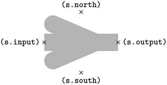
Shape generic diode IEC 
-
/pgf/generic diode IEC/before background=⟨code⟩(no default) 
This shape is used to depict diodes. The main shape is taken up by a “right pointing” triangle. The anchors are positioned on the border of a rectangle around the diode, see the below example. The diode’s size is based on the current settings of minimum width and minimum height.

                    \usetikzlibrary {circuits.ee.IEC}

                    \begin{tikzpicture}

                      \node[name=s,shape=generic diode IEC,shape example,minimum size=6cm] {};

                      \foreach \anchor/\placement in

                        {center/above, 30/above
                    right,

                         north/above, south/below, east/left, west/right,

                         north
                    east/above, south
                    east/below, south
                    west/below, north
                    west/above,

                         input/left,output/right}

                         \draw[shift=(s.\anchor)] plot[mark=x] coordinates{(0,0)}

                           node[\placement] {\scriptsize\texttt{(s.\anchor)}};

                    \end{tikzpicture}
This shape, like the generic circle IEC shape, is generic in the sense that there is a special key that is used for the before background drawings:
Similarly to the generic circle IEC shape, when a node of shape generic diode IEC is created, the current setting of this key is used as the “before background path”. When the ⟨code⟩ is executed, the coordinate system will have been transformed in such a way that the origin is at the “tip” of the diode’s triangle, the point \((0\mathrm {pt},1\mathrm {pt})\) is exactly half the diode’s height above this origin, and the point \((1\mathrm {pt},0\mathrm {pt})\) is half the diode’s height to the right of the origin.
The idea is that you use this key to draw different kinds of diode endings.
                        \usetikzlibrary {circuits.ee.IEC}

                        \tikz \node [minimum size=1cm,generic diode IEC,

                                     /pgf/generic diode IEC/before background={

                                         \pgfpathmoveto{\pgfqpoint{-.5pt}{-1pt}}

                                         \pgfpathlineto{\pgfqpoint{.5pt}{-1pt}}

                                         \pgfpathmoveto{\pgfqpoint{0pt}{-1pt}}

                                         \pgfpathlineto{\pgfqpoint{0pt}{1pt}}

                                         \pgfpathmoveto{\pgfqpoint{-.5pt}{1pt}}

                                         \pgfpathlineto{\pgfqpoint{.5pt}{1pt}}

                                         \pgfusepathqstroke

                                       },

                                     draw] {};
-
Shape breakdown diode IEC 
This shape is used to depict a bidirectional breakdown diode. The diode’s size is based on the current settings of minimum width and minimum height.
                    \usetikzlibrary {circuits.ee.IEC}

                    \begin{tikzpicture}

                      \node[name=s,shape=breakdown diode IEC,shape example,minimum width=6cm,minimum height=4cm] {};

                      \foreach \anchor/\placement in

                        {center/above, 30/above
                    right,

                         north/above, south/below, east/left, west/right,

                         north
                    east/above, south
                    east/below, south
                    west/below, north
                    west/above,

                         input/left,output/right}

                         \draw[shift=(s.\anchor)] plot[mark=x] coordinates{(0,0)}

                           node[\placement] {\scriptsize\texttt{(s.\anchor)}};

                    \end{tikzpicture}
-
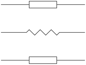
Shape var resistor IEC 
This shape is used to depict a variant version of a resistor. Its size is computed as for a rectangle (thus, its size depends things like the minimum height). Then, inside this rectangle, a background path is set up according to the following rule: Starting from the left end, zigzag segments are added to the path. Each segment consists of a line at a 45 degree angle going up to the top of the rectangle, then going down to the bottom, then going up to mid height of the node. As many segments as possible are put inside as possible. The last segment is then connected to the output anchor via a straight line.
All of this means that, in general, the shape should be much wider than high.
                    \usetikzlibrary {circuits.ee.IEC}

                    \begin{tikzpicture}

                      \node[name=s,shape=var resistor IEC,shape example,minimum width=7cm,minimum height=1cm] {};

                      \foreach \anchor/\placement in

                        {center/above, 30/above
                    right,

                         north/above, south/below, east/left, west/right,

                         north
                    east/above, south
                    east/below, south
                    west/below, north
                    west/above,

                         input/left,output/right}

                         \draw[shift=(s.\anchor)] plot[mark=x] coordinates{(0,0)}

                           node[\placement] {\scriptsize\texttt{(s.\anchor)}};

                    \end{tikzpicture}
-
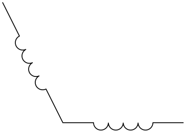
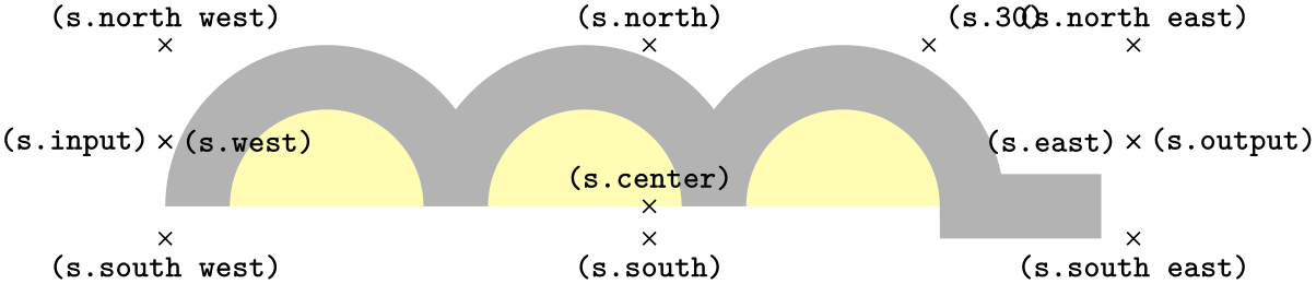
Shape inductor IEC 
This shape is used to depict an inductor, using a bumpy line. Its size is computed as follows: Any text and inner sep are ignored (and should normally not be given). The minimum height plus (twice) the outer ysep specify the distance between the north and south anchors, similarly for the minimum width plus the outer xsep for the east and west. The bumpy line is drawn starting from the lower left corner to the lower right corner with bumps being half-circles whose height is exactly the minimum height. The center of the shape is just above the south anchor, at a distance of the outer ysep.
                    \usetikzlibrary {circuits.ee.IEC}

                    \begin{tikzpicture}

                      \node[name=s,shape=inductor IEC,shape example,minimum width=7cm,minimum height=1cm] {};

                      \foreach \anchor/\placement in

                        {center/above, 30/above
                    right,

                         north/above, south/below, east/left, west/right,

                         north
                    east/above, south
                    east/below, south
                    west/below, north
                    west/above,

                         input/left,output/right}

                         \draw[shift=(s.\anchor)] plot[mark=x] coordinates{(0,0)}

                           node[\placement] {\scriptsize\texttt{(s.\anchor)}};

                    \end{tikzpicture}
Just as for a var resistor IEC, as many bumps as possible are added and the last bump is connected to the output anchor via a straight line.
-
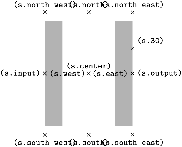
Shape capacitor IEC 
This shape is based on a rectangle ee. However, instead of a rectangle as the background path, only the “left and right lines” that make up the rectangle are drawn.
                    \usetikzlibrary {circuits.ee.IEC}

                    \begin{tikzpicture}

                      \node[name=s,shape=capacitor IEC,shape example,

                            minimum width=2cm,minimum height=3cm,inner sep=0pt] {};

                      \foreach \anchor/\placement in

                        {center/above, 30/above
                    right,

                         north/above, south/below, east/left, west/right,

                         north
                    east/above, south
                    east/below, south
                    west/below, north
                    west/above,

                         input/left,output/right}

                         \draw[shift=(s.\anchor)] plot[mark=x] coordinates{(0,0)}

                           node[\placement] {\scriptsize\texttt{(s.\anchor)}};

                    \end{tikzpicture}

-
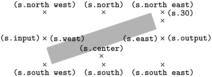
Shape make contact IEC 
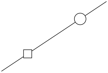
This shape consists of a line going from the lower left corner to the upper right corner. The size and anchors of this shape are computed in the same way as for an inductor IEC.

                    \usetikzlibrary {circuits.ee.IEC}

                    \begin{tikzpicture}

                      \node[name=s,shape=make contact IEC,shape example,minimum width=3cm,minimum height=1cm] {};

                      \foreach \anchor/\placement in

                        {center/above, 30/above
                    right,

                         north/above, south/below, east/left, west/right,

                         north
                    east/above, south
                    east/below, south
                    west/below, north
                    west/above,

                         input/left,output/right}

                         \draw[shift=(s.\anchor)] plot[mark=x] coordinates{(0,0)}

                           node[\placement] {\scriptsize\texttt{(s.\anchor)}};

                    \end{tikzpicture}
-
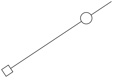
Shape var make contact IEC 
This shape works like make contact IEC, only a little circle is added to the path at the lower left corner. The radius of this circle is one twelfth of the width of the node.
                    \usetikzlibrary {circuits.ee.IEC}

                    \tikz \node[shape=var make contact IEC,shape example,

                                minimum height=1cm,minimum width=3cm,inner sep=0pt] {};
-
Shape break contact IEC 
This shape depicts a contact that can be broken. It works like make contact IEC.

                    \usetikzlibrary {circuits.ee.IEC}

                    \tikz \node[shape=break contact IEC,shape example,

                                minimum height=1cm,minimum width=3cm,inner sep=0pt] {};